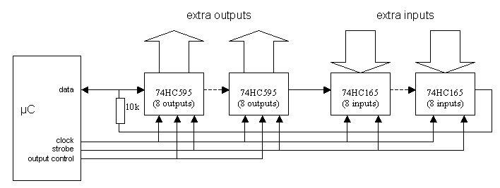
The shift register chain is made up of a number of output shift register devices (74HC595 or 74HC4094s) and a number of input shift register devices (74HC165). Both these chips are 8-bits wide, so the number of inputs and outputs available will be a multiple of 8. Only as many devices as are required may be fitted.
The circuit description covers use of the 74HC595. Use of the 74HC4094 (which may be cheaper and easier to find) is covered later in this document. First the strobe line is dipped low and back high again. This latches all the inputs into the 74HC165 input shift registers. Then the clocking begins. With each clock pulse, the data line is set to an output, and the appropriate data bit is presented on the line to be clocked into the output shift register. On the same clock pulse, the input shift register presents its next data bit to the microcontroller data pin. The data pin is set to an input, and this data bit read.
The number of clock pulses required is the larger of the number of inputs and the number of outputs. After this number of clock pulses, all the required output states have been shifted into position in the 74HC597 output shift registers, and another dipping of the "strobe" line is performed to set these states on the shift register output pins.
A timing diagram for this operation is shown below:
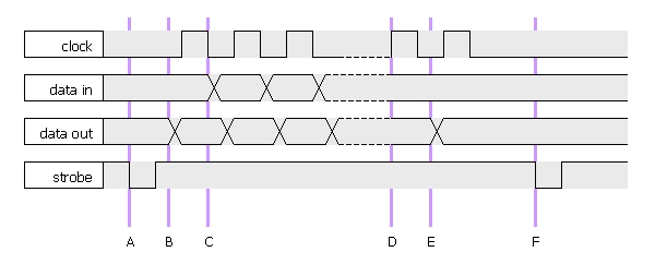
The points in this diagram are:
You can make the chain any length you want, with as many output stages or input stages as required. It may be all input stages, or it may be all output stages too. There are constants in the code where the dimensions of the shift register are defined, and they control how the software drives it.
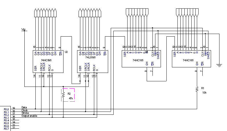
Click on the circuit diagram to open it in a new window.
R1 is the feedback resistor so the data pin can read the shift register and write to it. R2 causes the output shift register's outputs to be tri-state until the microcontroller code can start and set the output enable line high to turn off the output shift register outputs.
Any inputs that are not used should be tied either high or low. CMOS inputs should never be left floating since they can be switched by external noise which may cause the IC to draw a lot more current than is necessary.
The table below shows what pins should be replaced for what, and whether the active state is different:
| 74HC595 pin | 74HC4094 pin | Function | Active state swap? |
| 12: STcp | 1: STR | Strobe / storage register clock | No |
| 14: Ds | 2: D | Serial data input | No |
| 11: SHcp | 3: CP | Shift register clock | No |
| 15: Q0 | 4: Q0 | Parallel data outputs | No |
| 1: Q1 | 5: Q1 | ||
| 2: Q2 | 6: Q2 | ||
| 3: Q3 | 7: Q3 | ||
| 4: Q4 | 14: Q4 | ||
| 5: Q5 | 13: Q5 | ||
| 6: Q6 | 12: Q6 | ||
| 7: Q7 | 11: Q7 | ||
| 9: Q7' | 9: QS1 | Serial data output | No |
| not on 595 | 10: QS2 | Second serial data output | - |
| 13: /OE | 15: OE | Output enable | Yes |
| 10: /MR | not on 4094 | Master reset | - |
One correspondent wanted to use the 74HC4094 device, and the parallel port of a PC running Windows to drive the shift register chain. This presented its own problems which I thought may be relevant to share here. The email discourse is here.
The code is heavily documented and is not very complicated.
At the top of the source file are three definitions:
// These define the chain dimensions
#define CHAIN_LENGTH 24 /* Length of chain in bits */
#define NUM_OUTPUTS 16 /* Number of outputs in chain */
#define NUM_INPUTS 8 /* Number of inputs in chain */
This is where the dimensions of the shift register are defined.
The input and output pins in this code are defined as follows in a separate header file for controlling the hardware. All hardware-dependant values should be defined in a single file so if the code is ported to another processor, hopefully only one file will need changing - this is a common feature of embedded programs.
//----------------
//
// Extension shift register
//
//----------------
#define SR_DATA P8DR.0
#define SR_CLOCK P8DR.1
#define SR_STROBE P8DR.2
#define SR_INPUT P8DDR = b00011110
#define SR_OUTPUT P8DDR = b00011111
The SR_DATA, SR_CLOCK, and SR_STROBE definitions define the port pins (in this example port 8 pins 0, 1, and 2 of a Hitachi H8S), and two more definitions are given (actually code macros) for changing the SR_DATA port to an input or output. The binary values b00011110 are defined in a separate file - all 256 values defined in the file binary.h. Binary numbers are not native to C unfortunately, so I include this binary definition file in nearly all my embedded software projects.
The following functions are available to the outside world:
void UpdateChain(void);
void InitialiseShiftRegisterChain(void);
void ChainSetBit(int BitNumber, int State);
void ChainSetBitNow(int BitNumber, int State);
void ChainSetByte(int ByteNumber, unsigned char Value);
void ChainSetByteNow(int ByteNumber, unsigned char Value);
unsigned char ChainReadBit(int BitNumber);
unsigned char ChainReadBitNow(int BitNumber);
There are two ways of setting or reading bits - an immediate mode and a delayed mode. The immediate mode is if you want to read or set a single bit and it must happen immediately. The functions ChainSetBitNow() and ChainReadBitNow() will perform this function. However, using these functions will perform a full clocking cycle on the shift register of CHAIN_LENGTH clock operations. If you wanted to set three bits in one go, you wouldn't want to drive CHAIN_LENGTH x 3 cycle, so the delayed form functions ChainSetBit() and ChainReadBit() are used. These just set the bits to the desired state in the shadow register inside the microcontroller. Once all the required bit states have been defined, the UpdateChain() function is called, and this will perform CHAIN_LENGTH clock cycles, update the outputs, and read in the new set of inputs.
The InitialiseShiftRegisterChain() function simply clears all the outputs to zero, which may (or may not) turn off all devices driven by these outputs.
The outputs can be written to a byte at a time as well if required (for example, I use one output shift register to drive an 8-bit data bus to an LCD controller, so all communication with that is done a byte at a time). Again, there is an immediate form, ChainSetByteNow(), and a delayed form ChainSetByte() that allows other outputs to be set up before a call to UpdateChain().
The comments in the UpdateChain() function explain exactly how the I/O lines are driven to write the appropriate bits to the shift registers.
Obviously, the more shift register chips that are added to the chain, the slower will be the response time of writing outputs or reading inputs. If the time becomes too great for your application, you will either have to move the input or output that needs to be faster to a direct I/O line, or you can create a second register chain. If you have a second chain with the same number of input and output shift register chips, then the "output control", "clock" and "strobe" lines can be commoned for both chains, and just a separate "data" line used, one for each chain. The code will then have to be modified so that there are two sets of shadow registers, and the data read and data write lines in UpdateChain() must be doubled up to cope with the extra chain.
| Manufacturer | Device | Description | Philips Semiconductors | 74HC165 | 8-bit shift register with parallel inputs |
| 74HC595 | 8-bit shift register with parallel outputs | |
| 74HC4094 | 8-stage shift-and-store bus register |
[E5] "Circuit Cellar" article describing ways to increase I/O capability:
http://www.circuitcellar.com/library/details/0999/c99cd1.asp
The above as a single PDF file
[E2] JAL (Just Another Language) GNU compiler for the PIC range has a library for
driving shift register chains for extending the I/O
The JAL page