MOSFETs come in four different types. They may be enhancement or depletion mode, and they may be n-channel or p-channel. We are only interested in n-channel enhancement mode MOSFETs, and these will be the only ones talked about from now on. There are also logic-level MOSFETs and normal MOSFETs. We can use either type.
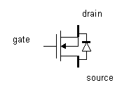
The source terminal is normally the negative one, and the drain is the positive one (the names refer to the source and drain of electrons). The diagram above shows a diode connected across the MOSFET. This diode is called the "intrinsic diode", because it is built into the silicon structure of the MOSFET. It is a consequence of the way power MOSFETs are created in the layers of silicon, and can be very useful. In most MOSFET architectures, it is rated at the same current as the MOSFET itself.
To examine the parameters of MOSFETs, it is useful to have a sample datasheet to hand. Click here to open a datasheet for the International Rectifier IRF3205, which we will be referring to. First we must go through some of the salient parameters that we will be dealing with.
This is the resistance between the source and drain terminals when the MOSFET is turned fully on.
This is the maximum current that the MOSFET can stand passing from drain to source. It is largely determined by the package and Rds(on).
This is the maximum power handling capability of the MOSFET, which depends largely on the type of package it is in.
This is how much the maximum power dissipation parameter above must be reduced by per ºC, as the temperature rises above 25ºC.
This is how much energy the MOSFET can withstand under avalanche conditions. Avalanche occurs when the maximum drain-to-source voltage is exceeded, and current rushes through the MOSFET. This does not cause permanent damage as long as the energy (power x time) in the avalanche does not exceed the maximum.
This is how fast the intrinsic diode can go from the off state (reverse biased) to the on state (conducting). It depends on how much voltage was across it before it turned on. Hence the time taken, t = (reverse voltage / peak diode recovery).
This is the maximum voltage that can be placed from drain to source when the MOSFET is turned off.
For more information on thermal resistance, see the chapter on heatsinks.
This is the minimum voltage required between the gate and source terminals to turn the MOSFET on. It will need more than this to turn it fully on.
As the gate-source voltage is increased, when the MOSFET is just starting to turn on, it has a fairly linear relationship between Vgs and drain current. This parameter is simply (Id / Vgs) in this linear section.
This is the lumped capacitance between the gate terminal and the source and drain terminals. The capacitance to the drain is the most important.
There is a more detailed introduction to MOSFETs in the International Rectifier Acrobat (PDF) document Power MOSFET Basics. This explains where some of the parameters come from in terms of the construction of the MOSFET.
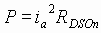
The power that the MOSFET will have to contend with is one of the major deciding factors. The power dissipated in a MOSFET is the voltage across it times the current going through it. Even though it is switching large amounts of power, this should be fairly small because either the voltage across it is very small (switch is closed - MOSFET is on), or the current going through it is very small (switch is open - MOSFET is off). The voltage across the MOSFET when it is on will be the resistance of the MOSFET, Rds(on) times the current going thorough it. This resistance, RDSon, for good power MOSFETs will be less than 0.02 Ohms. Then the power dissipated in the MOSFET is:
For a current of 40 Amps, RDSon of 0.02 Ohms, this power is 32 Watts. Without a heatsink, the MOSFET would burn out dissipating this much power. Choosing a heatsink is a subject in itself, which is why there is a chapter devoted to it:heatsinks.
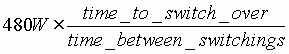
The on-resistance isn't the only cause of power dissipation in the MOSFET. Another source occurs when the MOSFET is switching between states. For a short period of time, the MOSFET is half on and half off. Using the same example figures as above, the current may be at half value, 20 Amps, and the voltage may be at half value, 6 Volts at the same time. Now the power dissipated is 20 × 6 = 120 Watts. However, the MOSFET is only dissipating this for the short period of time that the MOSFET is switching between states. The average power dissipation caused by this is therefore a lot less, and depends on the relative times that the MOSFET is switching and not switching. The average dissipation is given by the equation:
Solution: At 20kHz, there is a MOSFET switching occurrence every 25 microseconds (a switch on every 50 microseconds, and a switch off every 50 microseconds). Therefore, the ratio of switching time to total time is 1/25 = 0.04. The power dissipation when switching is (12v / 2) x (40A / 2) = 120 Watts. Therefore the average switching loss is 120W x 0.04 = 4.8 Watts.
Any power dissipation above about 1 Watt requires that the MOSFET is mounted on a heatsink. Power MOSFETs come in a variety of packages, but normally have a metal tab which is placed against the heatsink, and is used to conduct heat away from the MOSFET semiconductor.
![[Image]](pict9.gif)
The power handling of the package without an extra heatsink is very small. On some MOSFETs, the metal tab is connected internally to one of the MOSFETs terminals - usually the drain. This is a disadvantage as it means that you cannot fit more than one MOSFET to a heatsink without electrically isolating the MOSFET package from the metal heatsink. This can be done with thin mica sheets placed between the package and the heatsink. Some MOSFETs have the package isolated from the terminals, which is better. At the end of the day your decision is likely to be based in price however!
MOSFETs are generally advertised by their maximum drain current. The advertising blurb, and the features list on the front of the datasheet may quote a continuous drain current, Id, of 70 Amps, and a pulsed drain current of 350 Amps. You must be very careful with these figures. They are not the general average values, but the maximum the MOSFET will carry under the best possible circumstances. For a start, they are normally quoted for use at a package temperature of 25 ºC. It is highly unlikely when you are passing 70 Amps that the case will still be at 25ºC! In the datasheet there should be a graph of how this figure derates with increasing temperature.
The pulsed drain current is always quoted under switching conditions with the switching times in very small writing at the bottom of the page! This may be a maximum pulse width of a couple of hundred microseconds, and a duty cycle (percentage of time ON to OFF) of only 2%, which is not very practical. For more information about the current ratings of MOSFETs, have a look at this International Rectifier document.
If you cannot find a single MOSFET with a high enough maximum drain current, then you can connect more than one in parallel. See later for information on how to do this.
You will be using the MOSFET in a switched mode to control the speed of the motors. As we saw earlier, the longer that the MOSFET is in the state where it is neither on nor off, the more power it will dissipate. Some MOSFETs are faster than others. Most modern ones will easily be fast enough to switch at several tens of kHz, since this is nearly always how they are used. On page 2 of the datasheet, you should see the parameters Turn-On Delay Time, Rise Time, Turn-Off Delay Time and Fall Time. If these are all added up, it will give you the approximate minimum square wave period that could be used to switch this MOSFET: 229ns. This represents a frequency of 4.3MHz. Note that it would get very hot though because it would spend a lot of its time in the switching over state.
Problem: A full bridge speed controller circuit is designed to control a 12v motor. The switching frequency must be above the audible limit (20kHz). The motor has a total resistance of 0.12 Ohms. Choose suitable MOSFETs for the bridge circuit, within a reasonable price limit, and suggest any heatsinking that may be required. The ambient temperature is assumed to be 25ºC.
Solution: Lets have a look at the IRF3205 and see if it is suitable. First the drain current requirement. At stall, the motor will take 12v / 0.12 Ohms = 100 Amps. We will first make a guess at the junction temperature, at 125ºC We must find what the maximum drain current is at 125ºC first. The graph of figure 9 shows us that at 125ºC, the maximum drain current is about 65 Amps. Therefore 2 IRF3205s in parallel should be capable in this respect.
How much power will the two parallel MOSFETs be dissipating? Lets start with the power dissipation whilst ON and the motor stalled, or just starting. That is the current squared times the on-resistance. What is RDS(on) at 125ºC? Figure 4 shows how it is derated from its front-page value of 0.008 Ohms, by a factor of about 1.6. Therefore, we assume RDS(on) will be 0.008 x 1.6 = 0.0128. Therefore PD = 50 x 50 x 0.0128 = 32 Watts. How much of the time will the motor be either stalled or starting? This is impossible to say, so we will have to guess. 20% of the time is quite a conservative figure - it is likely to be a lot less. Since the power causes heat, and the heat conduction is quite a slow process, the effect of power dissipation tends to get averaged out over quite long time periods, in the region of seconds. Therefore we can derate the power requirement with the quoted 20%, to arrive at an average power dissipation of 32W x 20% = 6.4W.
Now we must add the power dissipated due to switching. This will occur during the rise and fall times, which are quoted in the Electrical Characteristics table as 100ns and 70ns respectively. Assuming the MOSFET driver can supply enough current to fulfill the requirements of these figures (gate drive source resistance of 2.5 Ohms = pulse output drive current of 12v / 2.5 Ohms = 4.8 Amps), then the ratio of switching time to steady-state time is 170ns * 20kHz = 3.4mW which is negligable. These on-off timings are a bit crude however, for more information about on-off times, see here.
Now what are the switching requirements? The MOSFET driver ship we use will cope with most of these, but its worth checking. The turn-on voltage, Vgs(th), from the graphs of Figure 3 is just over 5 Volts. We have already seen that the driver should be able to source 4.8 Amps for a very short period of time.
Now what about the heatsink. You may want to read the chapter on heatsinks before this section. We want to keep the temperature for the semiconductor junction below 125ºC, and we have been told that the ambient temperature is 25ºC. Therefore, with a MOSFET dissipating 6.4W on average, the total thermal resistance must be less than (125 - 25) / 6.4 = 15.6 ºC/W. The thermal resistance from junction to case makes up for 0.75 ºC/W of this, typical case to heatsink values (using thermal compound) are 0.2 ºC/W, which leaves 15.6 - 0.75 - 0.2 = 14.7 ºC/W for the heatsink itself. Heatsinks of this θjc value are quite small and cheap. Note that the same heatsink can be used for both MOSFETs to the left of or to the right of the load in the H- bridge, since these two MOSFETs are never both on at the same time, and so can never both be dissipating power at the same time. The cases of them must be electrically isolated however. See the heatsinks page for more information on the required electrical isolation.
To turn a power MOSFET on, the gate terminal must be set to a voltage at least 10 volts greater than the source terminal (about 4 volts for logic level MOSFETs). This is comfortably above the Vgs(th) parameter.
One feature of power MOSFETs is that they have a large stray capacitance between the gate and the other terminals, Ciss. The effect of this is that when the pulse to the gate terminal arrives, it must first charge this capacitance up before the gate voltage can reach the 10 volts required. The gate terminal then effectively does take current. Therefore the circuit that drives the gate terminal should be capable of supplying a reasonable current so the stray capacitance can be charged up as quickly as possible. The best way to do this is to use a dedicated MOSFET driver chip.
There are a lot of MOSFET driver chips available from several companies. Some are shown with links to the datasheets in the table below. Some require the MOSFET source terminal to be grounded (for the lower 2 MOSFETs in a full bridge or just a simple switching circuit). Some can drive a MOSFET with the source at a higher voltage. These have an on-chip charge pump, which means they can generate the 22 volts required to turn the upper MOSFET in a full brifge on. The TDA340 even controls the swicthing sequence for you. Some can supply as much as 6 Amps current as a very short pulse to charge up the stray gate capacitance.
| Manufacturer | IC | Features |
| Maxim and others | ICL 7667 | Dual inverting driver |
| Maxim | MAX622/MAX1614 | High side drivers |
| Maxim | MAX626/MAX627/MAX628 | Low side drivers |
| International Rectifier | IR2110 | High and low side driver |
| Harris / Intersil | HIP4080/4081/4082 | Full bridge drivers |
| SGS Thomson (ST) | TD340 | New full bridge driver with analogue or PWM speed demand input |
| Other manufacturers include: | Alpha semiconductor |
For more information on MOSFETs and how to drive them, International Rectifier has a set of technical papers on their HEXFET range here.
Often you will see a low value resistor between the MOSFET driver and the MOSFET gate terminal. This is to dampen down any ringing oscillations caused by the lead inductance and gate capacitance which can otherwise exceed the maximum voltage allowed on the gate terminal. It also slows down the rate at which the MOSFET turns on and off. This can be useful if the intrinsic diodes in the MOSFET do not turn on fast enough. More details of this can be found in the International Rectifier technical documents.
MOSFETs can be placed in parallel to improve the current handling capability. Simply join the Gate, Source and Drain terminals together. Any number of MOSFETs can be paralleled up, but note that the gate capacitance adds up as you parallel more MOSFETs, and eventually the MOSFET driver will not be able to drive them. Note that you cannot parellel bipolar transistors like this. The reasons behind this are discussed in a technical paper here.