V1.0 19-Dec-00
The function of the snubber network is to limit the rate of change of the voltage across the motor (out- put terminals of the L6203) when one of the DMOS devices is turned off. Using the RC snubbing circuit shown in figure 1, the rate of change of the voltage on the output is dominated by the capacitor while the resistor is used primarily to limit the peak current flowing through the power transistor when it turns on.
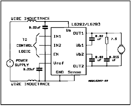
Figure 1 : DC Motor Drive Applications with Snubber Network and Bypass Capacitor.
The time constant of the motor current is much longer than the switching time, due to the inductance of the motor. At the time of switching the DC motor can be assumed to be a constant current generator equal to the peak current at switching. If this current is switched into the snubber, the voltage across the snubber network will jump to a value equal to the snubber resistance times the motor current. After the initial step, the rate of change is limited by the motor current charging the snubber capacitor.
To properly size the snubber network the resistor is selected such that the maximum motor current will produce a voltage less than the minimum power supply voltage. If the resistor is larger than this value, the snubber will be ineffective since the capacitor will not limit the voltage rise until the voltage has become greater than the power supply. For the design example, the maximum resistance for the snubber is given by the equation :
![]()
The snubber capacitor is calculated from the peak current and the target rise time. The capacitance is given by the equation:
![]()
When the snubber network is installed in the application the voltage transients on the terminals of the L6203 are greatly reduced, as shown in figure 2. The drawback of a snubber network of this type is that a current spike will flow into the transistor when it is switched on as the capacitor is discharged. The theoretical peak value of this spike is given by the equation :
![]()
The following graphs are of operating voltages with snubber network and bypass capacitor.
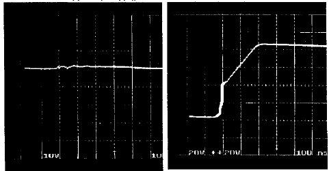
Figure 2a : Supply Voltage. Figure 2b : Vout1 - Vout2.
This peak current flowing in the snubber is added to the load current when the device is turned on and the total peak current in the transistor is the sum of the snubber circuit current plus the load current. In practice the peak current measured is usually much less than the calculated peak, due to the capacitors internal resistance and inductance and the resistor inductance. Figure 3 shows the peak current in the snubber network in the design example.
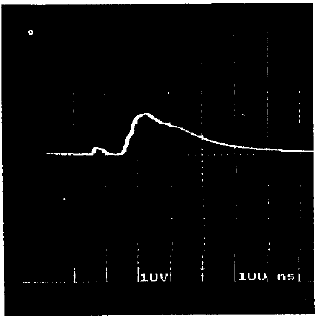
Figure 3: Current in the Snubber Circuit at turn on (2.0A/div)
The power dissipated in the snubber resistor is the sum of the dissipation during the turn-on and turn-off of the bridge. The resistor dissipation is :
![]()
where:
I1 = Current at turn-on
I2 = Current at turn-off
R = Snubber resistor
DC = Duty Cycle of current flow
For the design example the power dissipation, not considering the duty cycle is :
Pd = 2.344 W