Testing status: Untested
The purpose of a servo reverser is to invert the PWM request signal such that an input low-value is translated into an output high-value, and an input high- value is translated into an output low-value.
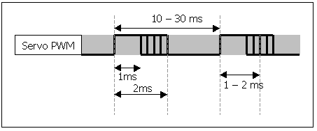
First we must see what these servo signals look like. There is a document here which describes servo signals in some detail, but I’ll reproduce the timing diagram here for simplicity.
A positive-going pulse is sent at regular intervals, at most every 30ms although some manufacturers have a maximum of 20ms between pulses. The width of the pulse is between 1ms and 2ms. A 1ms pulse will cause the servo to turn to its minimum extremity, and a 2ms pulse will cause it to turn to its maximum extremity. The range is linear, which means the centre-point the servo position is achieved by sending 1.5ms, halfway between 1ms and 2ms.
A table can be drawn of the servo position compared with the pulse width that causes that position:
Servo position |
Pulse width |
0% |
1ms |
20% |
1.2ms |
40% |
1.4ms |
50% |
1.5ms |
60% |
1.6ms |
80% |
1.8ms |
100% |
2ms |
This relationship is easy to show as an equation which can then be graphed:
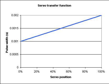
PW = 1 + (P÷100) To this graph, we can add the response that we want the output of our servo reverser to have (in red):
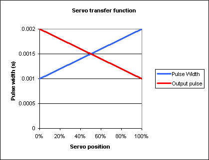
The equation of this red output line is:
PW = 2 - (P÷100)
Adding another column to the table will show us what output pulse widths we need from the circuit:
Servo position |
Pulse width |
Output pulse width |
0% |
1ms |
2ms |
20% |
1.2ms |
1.8ms |
40% |
1.4ms |
1.6ms |
50% |
1.5ms |
1.5ms |
60% |
1.6ms |
1.4ms |
80% |
1.8ms |
1.2ms |
100% |
2ms |
1ms |
Let’s look at some example timing diagrams:
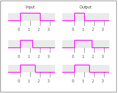
The output pulse width can be expressed in terms of the input pulse width with the following equation:
Pwout = 2ms - ( PWin – 1ms)
=> PWout = 3ms - PWin
The idea is to have a 3ms reference pulse, and subtract the input pulse from it:
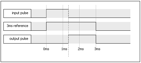
It can be seen from the timing diagram above that the output pulse waveform can be obtained from the other two waveforms by the logic equation:

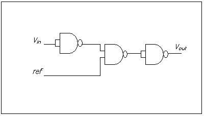
(where a dot means "logical AND" and an overhead bar means " inverted"). We could implement this using a quad NAND logic IC as follows:
This functionality can be also be performed with a couple of transistors if you prefer. Note that if you are using surface mount ICs however, a single 74HC00 quad NAND gate IC will probably take up less space on the circuit board than this discrete version:
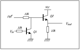
In this circuit, the reference pulse is passed straight on via the follower Q2. However, when the input pulse is present, Q1 is turned on, which clamps the base of Q2 to ground, thereby turning it off. Note that the high-level output of this circuit will be about 0.8 volts lower than Vcc, i.e. 4.2 volts of using standard logic power supplies.
Personally, I would use the 74HC00 quad NAND since this is easier all round.
The reference pulse is obtained using the 74HC123 dual monostable. This can be configured to generate a positive or negative going pulse of a fixed width, and can be triggered by a rising or falling edge input. Here, it is configured to generate a positive
going pulse triggered by a positive going input edge. The pulse from the radio receiver triggers it, and it's output will then go high for a period of 3ms, after which it will go low again.
The width of the output pulse of the monostable is determined by a resistor and capacitor value, and is simply
t = RC
We can now take all these blocks that we have designed, and merge them into one circuit. The completed circuit is shown in the diagram below:
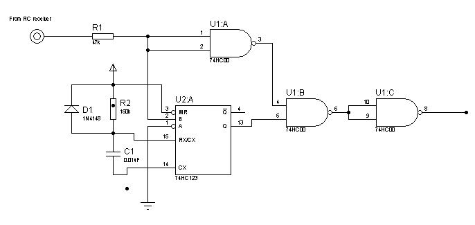
To make the 3 milliseconds as accurate as possible, it is recommended to use 1% tolerance resistors and capacitors. Vishay make a range of low-tolerance capacitors (see parts list at the bottom of this page). 1% resistors are easy to come by. The diode across the resistor (D1) is to prevent excessive currents in the chip.
Any unused inputs on both the 74HC123 and the 74HC00 should be tied to a fixed voltage (Gnd or Vcc).
Since the 74HC123 is a dual monostable, a dual channel servo reverser can easily be made with the addition of another 74HC00.
The following devices are used in this circuit. Click on the device name to go to the datasheet. Click on the manufacturer’s name to go to their website.
| Manufacturer | Device and datasheet link | Approximate cost |
| Vishay-Roederstein | MKP 1837 1% polypropylene capacitors | £0.80 |
| Philips Semiconductor | P74HC123 monostable | £0.30 |
| P74HC00 Quad NAND gate | £0.30 | |
| Fairchild Semiconductor | 1N4148 Signal diode | £0.10 |
I must thank Brent Dane for the thinking behind this, if not for the implementation. I was fixed on the idea that the output pulse to the servo must start at the same point in time as the input pulse from the receiver, which caused my initial design to be grossly over-complicated. Brent’s circuit uses a NE556 (dual NE555) timer IC to perform the same functionality as I do here with a dual monostable, 74HC123. His can be found here: http://www.cliftech.com.