V6.00 3-Aug-04
Testing status: Simulated.
The signal output by the radio control receiver is a form of PWM. This may be useful for driving servos, but is inconvenient for general electronic applications. Therefore, several of the circuits on this site convert this signal into a voltage first. This is performed by this circuit. It is not a project in its own right, just a building block used by other projects.
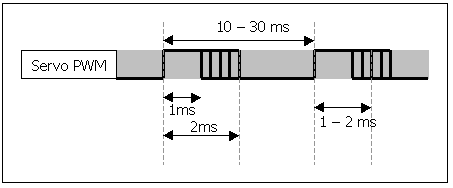
First we must see what these signals look like. There is a document here which describes servo signals in some detail, but I’ll reproduce the timing diagram here for simplicity.
A positive-going pulse is sent at regular intervals, at most every 30ms although some manufacturers have a maximum of 20ms between pulses. The width of the pulse is between 1ms and 2ms. A 1ms pulse will cause the servo to turn to its minimum extremity, and a 2ms pulse will cause it to turn to its maximum extremity. The range is linear, which means the centre-point the servo position is achieved by sending 1.5ms, halfway between 1ms and 2ms.
As a point of information, there is a good reason for the space between each pulse. On a multi-channel transmitter, there will be other pulses interspersed between the pulses shown. For example, a four channel system will have pulses for each channel sent in sequence: 1 - 2 - 3 - 4 - 1 - 2 - 3 - 4 etc. There will be a gap larger than 2ms between pulse 4 and pulse 1 to tell the receiver that the sequence is about to restart and the next pulse is pulse 1. The gap between the other pulses is less than 2ms. The receiver therefore knows which pulse comes next, and can direct it to the appropriate servo output. Therefore the waveform shown above is for just one servo channel.
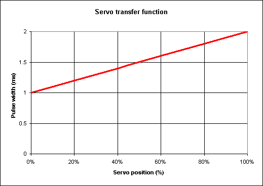
A table can be drawn of the servo position compared with the pulse width that causes that position:
servo position |
pulse width |
0% |
1ms |
20% |
1.2ms |
40% |
1.4ms |
50% |
1.5ms |
60% |
1.6ms |
80% |
1.8ms |
100% |
2ms |
This relationship is easy to show as an equation which can then be graphed:
PW = 1 + (P ÷ 100)
There are two ways of decoding the signal, one analogue, and one digital. Which is done depends really on the circuit that this sub-circuit is part of. Both methods are described here, and where this sub-circuit is used, the appropriate type is selected.
The width of the input pulse must be measured, and converted from milliseconds into volts. Therefore we must generate an output voltage that varies between 1V and 2V.
This is performed using a voltage ramp:
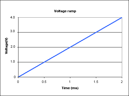
The slope of the ramp is approximately 2 Volts per millisecond, although it is not that critical as long as the circuit that interprets this voltage knows what the voltages are that represent 1ms and 2ms.
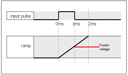
The idea is to start the ramp going when the pulse arrives.When the pulse finishes, we freeze the voltage of the ramp. This frozen value will be the output of the circuit:
A linear ramp like this is generated by charging a capacitor with a constant current. Here’s the maths of it, skip it if you’re not interested:
Maths of linear ramps
The relationship between the voltage across, and current flowing through a capacitor is given by the equation:

where t = time, and C = capacitance.
If the current, i, is constant then the equation simplifies to:

Therefore if the current is kept constant, as t increases linearly (we hope!), then the voltage on the capacitor will increase linearly too.
We want a constant current source to start charging the capacitor when the pulse arrives, and continue charging it after the pulse has gone. A simple current source is shown in the circuit below:
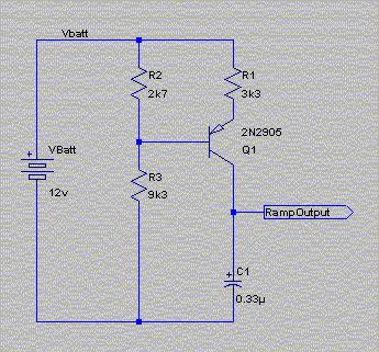
This circuit is a constant current source charging a capacitor. The two biasing resistors R2 and R3 fix the base of the transistor at a voltage equal to
12V × R3 ÷ (R2 + R3) = 9.3V.
The transistor Vbe is approximately 0.7V. Therefore the transistors emitter must be fixed at a voltage of 9.3V + 0.7V = 10V. Since both ends of R1 are at fixed voltages, then the current flowing through it must be fixed:
I(R1) = (12V - 10V) ÷ 3k3 = 606uA.
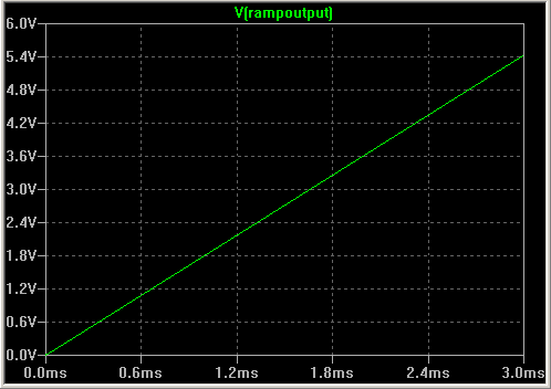
We have seen above that a constant current charging a capacitor results in a constantly rising voltage. Here's a result of a SPICE simulation of this circuit:
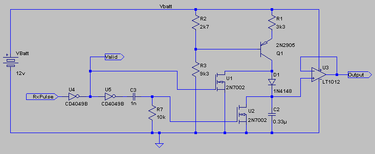
We want the ramp to start charging when the pulse from the radio receiver arrives. This is a bit tricky, because we need the voltage on the capacitor to be reset to zero when the pulse arrives, and then be allowed to charge up. To achieve this, the voltage on the capacitor is reset to zero by momentarily switching on a MOSFET (U2) placed across the capacitor.
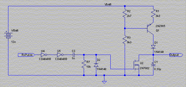
The MOSFET must only be turned on for a very short time - enough time to short out and discharge the capacitor, but not long enough to adversely delay the charging up of the capacitor. A voltage spike is generated to achieve this. First the pulse from the receiver (blue trace in simulation below) is squared up using the CMOS inverter gates U4 and U5 (these are 2 out of the 6 gates in one 4049 chip). The RC network C3-R7 then creates a high going spike on the rising edge of the pulse, and a low-going spike on the falling edge of the pulse (red trace in simulation):
The diode D2 is there to prevent the negative going spike taking the MOSFET gate-source voltage too far negative and destroying the MOSFET. However, the 2N7002 Vgs maximum rating is ±20V, so there is no need for this diode and it is not present in the final design.
The high-going spike is enough to turn on the MOSFET momentarily, which shorts out the capacitor, setting the output voltage to zero. The constant current source then continues to charge it up (see green trace in simulation).
Now we want the capacitor to stop charging, and just hold its current voltage when the input pulse goes low again. This is achieved by diverting the current from the constant current source through a second MOSFET when the input pulse is low:
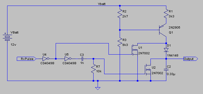
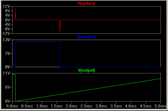
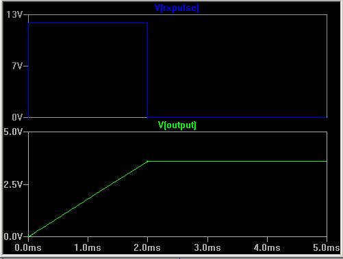
The MOSFET U1 turns on when the pulse from the receiver goes low. This diverts the current from the constant current source through U1. Notice the addition of the diode D1. This still allows the capacitor to be charged, but prevents U1 shorting out the capacitor. The simulation below shows the output voltage charging, then stopping at a fixed voltage when the pulse returns low:
The final addition to the circuit is to buffer the output. Without a buffer, if any circuits that use the output of this circuit pull any current at all, this will discharge the capacitor, and the output voltage will droop. The addition of the buffer opamp (U3) prevents this:
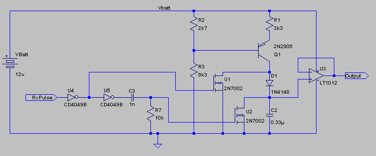
The opamp chosen has a very low input bias current, which means it hardly takes any current from the capacitor, resulting in a stable voltage. This particular opamp (LT1014) only works from about a volt above its negative rail, which means the output can never be less than about 1V, but the minimum output we would expect is for a 1ms wide input pulse, which gives an output voltage of about 2V anyway. Therefore we do not need to worry about it.
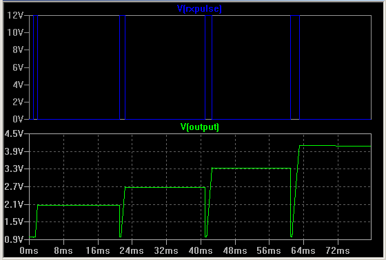
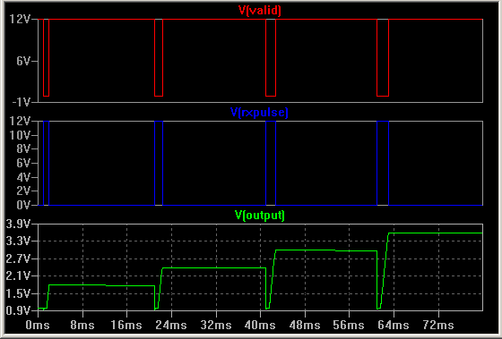
This final simulation shows the output given a stream of input pulses of widths 1.0ms, 1.33ms, 1.67ms, and 2.0ms:
Note that the output voltage is only valid between the received pulses. This could cause a problem if a following circuit tries to use the voltage when a pulse is in the process of arriving. We can supply a 'Valid' signal to tell any following circuit when the output voltage is valid. This is simply the inverse of the received pulse, which is available at the output of U4:
Instead of relying on a 'Valid' signal like this, the voltage on the capacitor could be simply low pass filtered to smooth over the times that the pulse is being measured. The following circuit has a simple RC low pass filter (R4 + C1) with a time constant of about 9 milliseconds. This is enough to get rid of most of the discontinuity without affecting the response of the circuit too much:
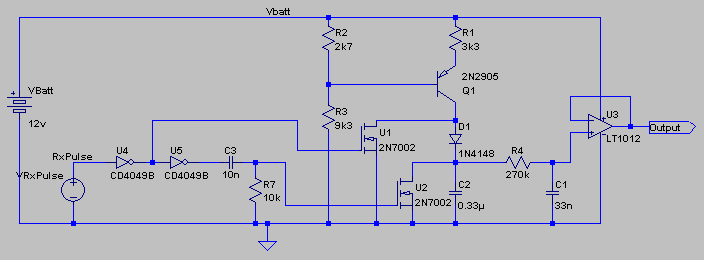
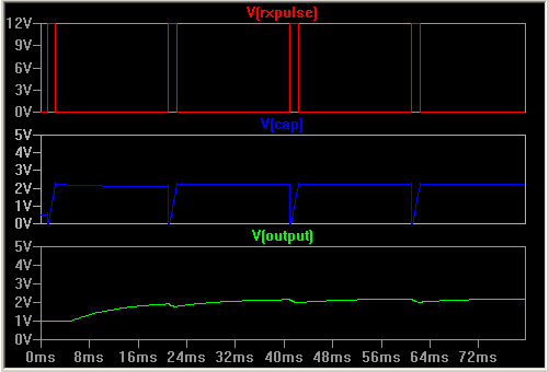
The effect on the output can be seen in this simulation showing four pulses all of 1.4ms duration. The output quickly stabilises at around the correct voltage. If it is required that the output be smoother, at the expense of response time, the time constant of the RC filter may be increased by increasing the values of R4 and C1.
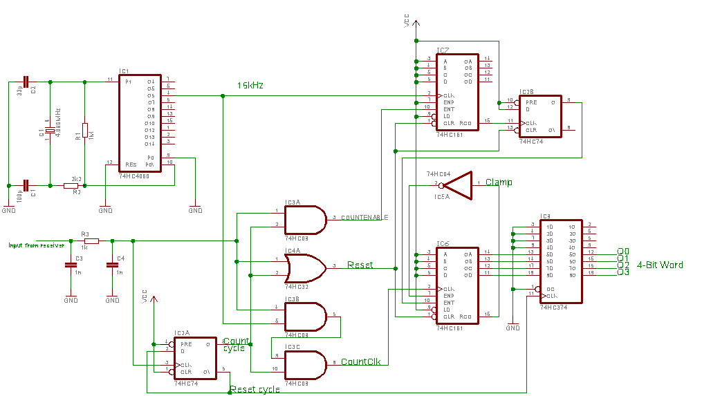
Click on the circuit diagram to open it in a new window.
The counters IC6 and IC7 are clocked off a frequency which has been selected such that there are 16 counts in 1 millisecond (1 period is 62.5us, so frequency is 16kHz). This has been achieved by dividing a 4.096MHz crystal by 256, which is easy using the 74HC4060 (IC1) oscillator-divider IC.
Since the incoming pulse is always between 1ms and 2ms, IC7 is clocked for the first 1ms, and then IC6 is enabled to be clocked for the remainder of the time that the incoming pulse is high.
The timing of the control signals is shown below for an input pulse width of 1.5 milliseconds:
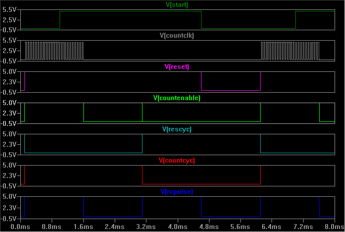
When the IC2a Q output is high and the RC pulse arrives, the counters count, and when the IC2a Q output is low and the RC pulse arrives, the count is latched by the octal D-type flip-flop, 74HC374 (IC8), and the counters and IC2b flip-flop are reset.
In the count cycle, the signal CountCyc is high, and IC3a then uses the input pulse to enable the IC7 counter. This counts sixteenths of milliseconds for the first millisecond of the input pulse. When its count reaches 15, its RCO output goes high and latches IC2b on. IC2b Q output is called "Start". When this goes high, it enables the IC6 counter. The IC6 counter is used to measure how far between 1ms and 2ms the pulse is wide. If the pulse is less than 1ms (an illegal value), then IC6 will still be at a count of 0000.
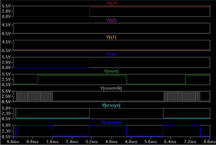
As soon as "Start" goes high, IC6 starts counting the "CountClk" signal counts. In a counting cycle, these will be at 16kHz. For the 1.5ms pulse width in the timing diagram, the counter will count up to 8 or 9 (depending on exactly how wide the pulse was). This count value is latched into IC8 (74HC374) when the "ResetCycle" signal goes high.
The following timing diagram shows the count value of 9 (binary 1001) appearing on the Q outputs of the circuit at this time:
If the pulse lasted for longer than 2ms, then the RCO output of IC6 will go high when it reaches 15 (binary 1111). IC5a then inverts this and uses it as a counter enable signal. Therefore, when the count reaches 15, it is not allowed to count any higher, and so an the output will clamp at a maximum of 15.
The following table shows the output of this circuit for various pulse input widths:
Rx pulse width |
4-bit word output |
<1.0 |
0 0 0 0 |
1.0 |
0 0 0 1 |
1.1 |
0 0 1 1 |
1.2 |
0 1 0 0 |
1.3 |
0 1 1 0 |
1.4 |
1 0 0 0 |
1.5 |
1 0 0 1 |
1.6 |
1 0 1 1 |
1.7 |
1 1 0 0 |
1.8 |
1 1 1 0 |
1.9 |
1 1 1 1 |
2.0 |
1 1 1 1 |
>2.0 |
1 1 1 1 |
The input signal to this circuit is coming from the RC receiver module at an unknown output voltage, through wires which may be wrapping around the robot picking up noise along the way. Therefore, this line should be appropriately conditioned first. If the RC receiver that you are using produces outputs which do not swing up to the 5V required of the CMOS chips in this circuit (for example it may contain TTL logic), then IC2, IC3 and IC4 should be replaced with the 74HCT equivalents. These will work with TTL input level signals (in which logic high may be as low as 2.7V). Unfortunately, use of 74HCT devices will make the input more prone to noise, so only do this if your RC receiver is delivering low voltage logic highs.
The input requires some filtering to screen out noise spikes that may be picked up along the way. Since this input is used as a clock to the flip-flop that controls whether the circuit is measuring or latching, any glitch on it will result in the circuit performing the wrong operation. The low pass input filter is a Pi-network:
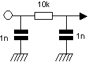
This filter has a 3dB point at about 16kHz (period 0.06ms). Lowering the cutoff frequency would improve the noise immunity but would shallow the rising and falling edge, and since we are measuring the width of this signal that is not a good idea. If the pulse shape is adversely affected, reduce the series resistor to 1k as in the circuit diagram.
The following devices are used in this circuit. Click on the device name to go to the datasheet. Click on the manufacturer’s name to go to their website.
Manufacturer |
Device and datasheet link |
4049B Hex inverting buffer |
|
74HC4060 Counter/divider |
|
74HC161 Dual 4-bit counter |
|
74HC374 Octal flip-flop |
|
74HC74 Dual D-type flip-flop |
|
74HC04 Hex inverter |
|
74HC08 Quad AND gate |
|
74HC32 Quad OR gate |
|
2N7002 N-channel MOSFET |
|
2N2905 PNP transistor |
LT1012 opamp |
Back to circuits index
Back to main index